General Description
The RT5716 is a synchronous buck converter with 4MHz typical switching frequency. This document only specifies the RT5716 in WL-CSP package. It explains the function and operation of the RT5716 evaluation board (EVB) and provides information about the setting of the evaluation board.
Performance Specifications
Performance specifications of the RT5716 are listed in Table 1.
(VIN = 3.6V, CIN = 4.7µF, COUT = 4.7µF x 2, L = 0.47µH, TJ = -40°C to 125°C, typical values are at TJ = 25°C, unless otherwise specified)
Table 1. Performance Specifications of the RT5716
|
Parameter
|
Symbol
|
Test Conditions
|
Min
|
Typ
|
Max
|
Unit
|
|
Supply Input Voltage
|
VIN
|
|
1.8
|
--
|
5.5
|
V
|
|
Output Current
|
IOUT
|
VIN ≥ 2.3V
For RT5716P-ABA, RT5716P-BBA, RT5716P-CBA, RT5716P-DBA
|
--
|
--
|
1
|
A
|
|
VIN < 2.3V
For RT5716P-ABA, RT5716P-BBA, RT5716P-CBA, RT5716P-DBA
|
--
|
--
|
0.7
|
A
|
|
Switching Frequency
|
fSW
|
|
--
|
4
|
--
|
MHz
|
|
Quiescent Current into VIN Pin (Non-Switching)
|
IQ_IN-NONSW
|
EN = VIN, VOUT = 1.2V, IOUT = 0A, RSEL/MODE = GND, TJ = -40°C to 85°C
|
--
|
2.3
|
3.7
|
µA
|
|
Quiescent Current into VIN Pin (Switching)
|
IQ_IN-SW
|
EN = VIN, VOUT = 1.2V, IOUT = 0A, RSEL/MODE = GND
|
--
|
2.5
|
--
|
|
Shutdown Current
|
ISHDN
|
EN = GND, RSEL/MODE = GND,
TJ = -40°C to 85°C
|
--
|
55
|
290
|
nA
|
Power-Up Procedure
Equipment Required
- RT5716 Evaluation Board
- DC power supply capable of at least 5.5V and 3A
- Electronic load capable of 1A
- Function Generator
- Oscilloscope
Quick Start Procedures
The evaluation board is fully assembled and tested. Follow the steps listed below to verify its functionality. Do not turn on power supplies until all equipment is well-connected. Do not measure the output voltage ripple with a long ground lead on the oscilloscope probe. Instead, touch the probe tip and ground ring directly across the output capacitor.
The setup procedures are listed below.
1) Connect JP21 so that the resistor is connected between the RSEL/ MODE pin and GND to set output voltage level.
2) Connect the power supply to VIN and GND pins and the electronic load to the VO and nearest GND pins before power on.
3) Turn on the input power supply and make sure that the input voltage does not exceed 5.5V.
4) Enable/disable the RT5716 by the EN pin. When the EN pin is higher than the threshold voltage of logic-high, the IC operates at normal mode; When the EN pin goes low, the RT5716 enters shutdown mode. In shutdown mode, the converter stops switching, internal control circuitry is turned off and discharge function is triggered.
5) When RT5716 starts up, the RSEL/MODE pin operates as an input used for mode selection. When connecting the RSEL/MODE pin to L, the RT5716 operates at Auto Mode, which is PFM mode; On the other hand, the RT5716 operates at FPWM mode when connecting the RSEL/MODE pin to H.
6) Check the output voltage by a voltmeter.
7) Adjust the load within the operating range and measure the output voltage regulation, ripple voltage, power efficiency and other performances.
Detailed Description of Hardware
Headers Description and Placement
Carefully inspect all the components used on the EVB according to the following Bill of Materials table, and make sure all the components are undamaged and correctly installed. If there is any missing or damaged component, which may occur during transportation, please contact our distributors or e-mail us at evb_service@richtek.com.
Test Points
The test points and pin names are listed in the table below.
|
Test Point/
Pin Name
|
Function
|
|
VIN
|
Input voltage.
|
|
VO
|
Output voltage.
|
|
GND
|
Ground.
|
|
EN
|
Enable pin.
|
|
RSEL/MODE
|
Output voltage level and operation mode selection pin.
|
Bill of Materials
RT5716P-ABA/RT5716P-BBA/RT5716P-CBA/RT5716P-DBA
|
Reference
|
Qty
|
Part Number
|
Value
|
Description
|
Package
|
Manufacturer
|
|
U1
|
1
|
RT5716P-ABA
RT5716P-BBA
RT5716P-CBA
RT5716P-DBA
|
RT5716
|
Step-Down Converter
|
TWL-CSP-6B 0.69x1.04 (BSC)
|
RICHTEK
|
|
C3, C4, C5
|
3
|
GRM155R60J475ME47D
|
4.7µF
|
Capacitor, Ceramic, 6.3V, X5R
|
0402
|
Murata
|
|
C9
|
1
|
GRM21BC80J476ME01
|
47µF
|
Capacitor, Ceramic, 6.3V, X6S
|
0805
|
Murata
|
|
L1
|
1
|
DFE18SANR47MG0L
|
0.47µH
|
0.47µH
|
0603
|
Murata
|
|
JP21
|
16
|
RC0201FR-0710KL
(Resistor E96 series)
|
Refer to Table 2
|
1%, TC ±200ppm
|
0201
|
YAGEO
|
Output Voltage Selection
The RT5716 provides 1 fixed and 16 different levels of VOUT which can be set by an external resistor connected between the RSEL/MODE pin and GND. Table 2 indicates the setting to different output voltage level.
Table 2. Output Voltage Setting
|
Type
|
Output-1 (V)
|
Output-2 (V)
|
Output-3 (V)
|
Output-4 (V)
|
RSEL (kW) *
|
|
Level
|
0.4V to 3.3V
|
0.4V to 0.775V
|
0.8V to 1.55V
|
1.8 V to 3.3V
|
Min
|
Nom
|
Max
|
|
0
|
3.3
|
0.7
|
1.2
|
1.8
|
Connected to GND
(No resistor needed)
|
|
1
|
0.4
|
0.4
|
0.8
|
1.8
|
9.9
|
10
|
10.1
|
|
2
|
0.58
|
0.425
|
0.85
|
1.9
|
12
|
12.1
|
12.2
|
|
3
|
0.6
|
0.45
|
0.9
|
2
|
15.2
|
15.4
|
15.6
|
|
4
|
0.7
|
0.475
|
0.95
|
2.1
|
18.5
|
18.7
|
18.9
|
|
5
|
0.75
|
0.5
|
1
|
2.2
|
23.5
|
23.7
|
23.9
|
|
6
|
0.8
|
0.525
|
1.05
|
2.3
|
28.4
|
28.7
|
29
|
|
7
|
1.1
|
0.55
|
1.1
|
2.4
|
36.1
|
36.5
|
36.9
|
|
8
|
1.2
|
0.575
|
1.15
|
2.5
|
43.8
|
44.2
|
44.6
|
|
9
|
1.3
|
0.6
|
1.2
|
2.6
|
55.6
|
56.2
|
56.8
|
|
10
|
1.5
|
0.625
|
1.25
|
2.7
|
67.4
|
68.1
|
68.8
|
|
11
|
1.6
|
0.65
|
1.3
|
2.8
|
85.7
|
86.6
|
87.5
|
|
12
|
1.8
|
0.675
|
1.35
|
2.9
|
104
|
105
|
106.1
|
|
13
|
1.9
|
0.7
|
1.4
|
3
|
131.7
|
133
|
134.3
|
|
14
|
2.5
|
0.725
|
1.45
|
3.1
|
160.4
|
162
|
163.6
|
|
15
|
3
|
0.75
|
1.5
|
3.2
|
203
|
205
|
207.1
|
|
16
|
3.3
|
0.775
|
1.55
|
3.3
|
³249
|
³249
|
³249
|
*: E96 resistor series, 1% accuracy, temperature coefficient better or equal than ±200 ppm/°C.
Typical Applications
EVB Schematic Diagram
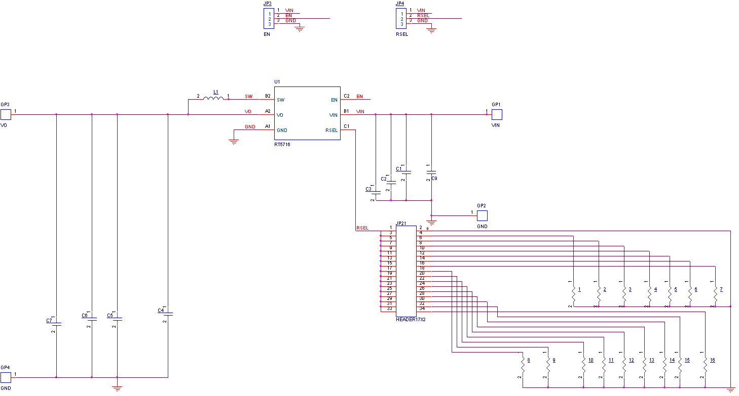
1. The capacitance of the input and output will influence the input and output voltage ripple, respectively.
2. MLCC capacitance degrades at different DC bias voltage. The smaller package size of MLCC capacitors, the more capacitance degradation there would be under the same test condition.
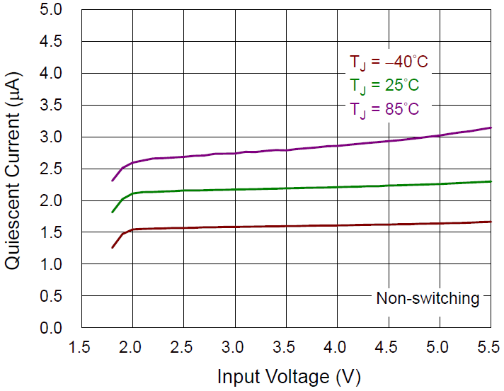
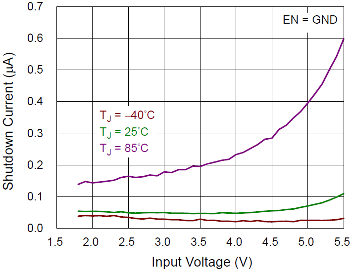
Measure Result
The following curves and waveforms are the measure results of the RT5716P-ABA.
|
Quiescent Current vs. Input Voltage
|
Shutdown Current vs. Input Voltage
|
|
|
|
|
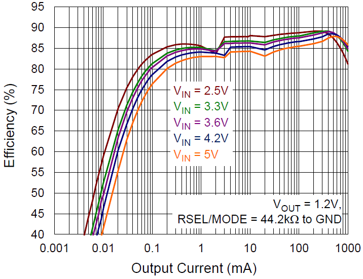
Efficiency vs. Output Current
|
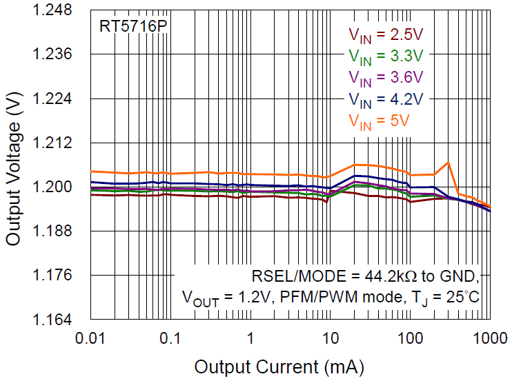
Output Voltage vs. Output Current
|
|
|
|
|
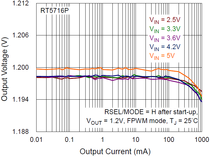
Output Voltage vs. Output Current
|
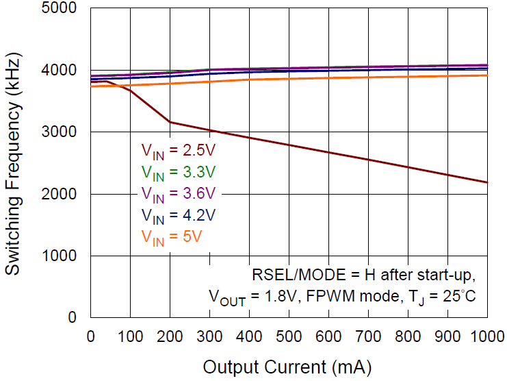
Switching Frequency vs. Output Current
|
|
|
|
|
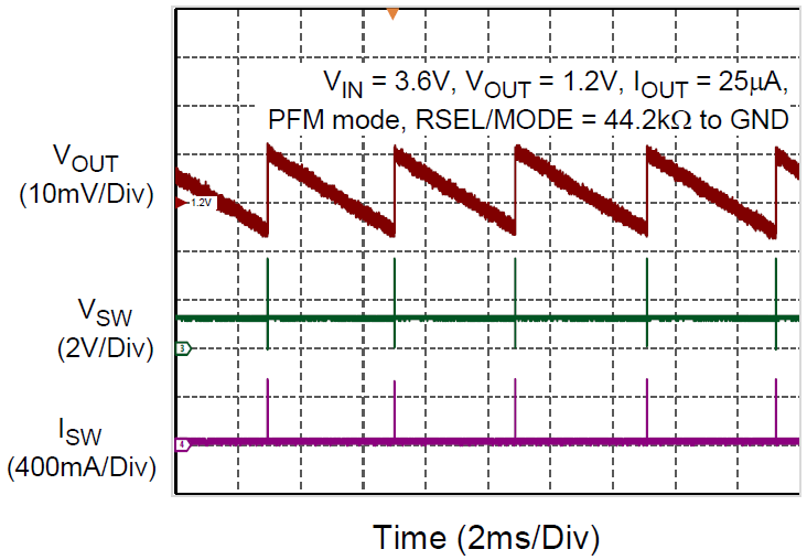
Power Save Mode Operation
|
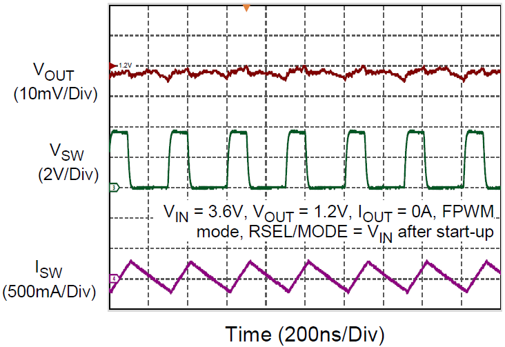
Pulse Width Modulation Operation
|
|
|
|
|
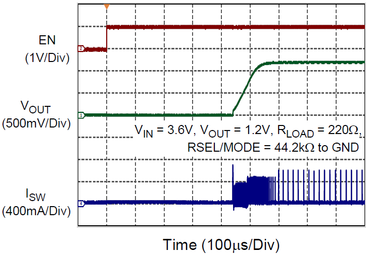
Power On with Light Load
|
AC Load Sweep at Power Save Mode
|
|
|
|
|
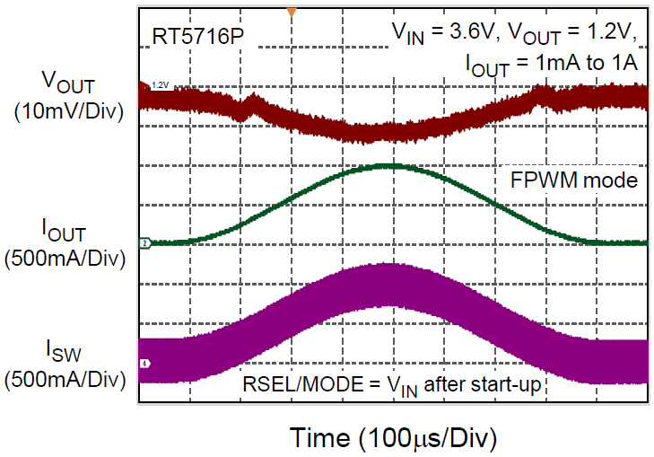
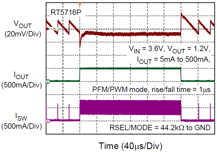
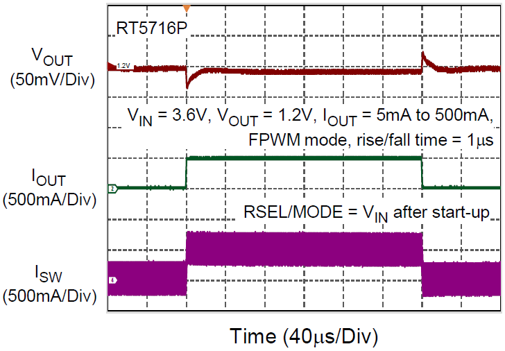
Load Transient Response
|
Load Transient Response
|
|
|
|
Note: Do not measure the output voltage ripple with a long ground lead on the oscilloscope probe. Instead, touch the probe tip and ground ring directly across the output capacitor.
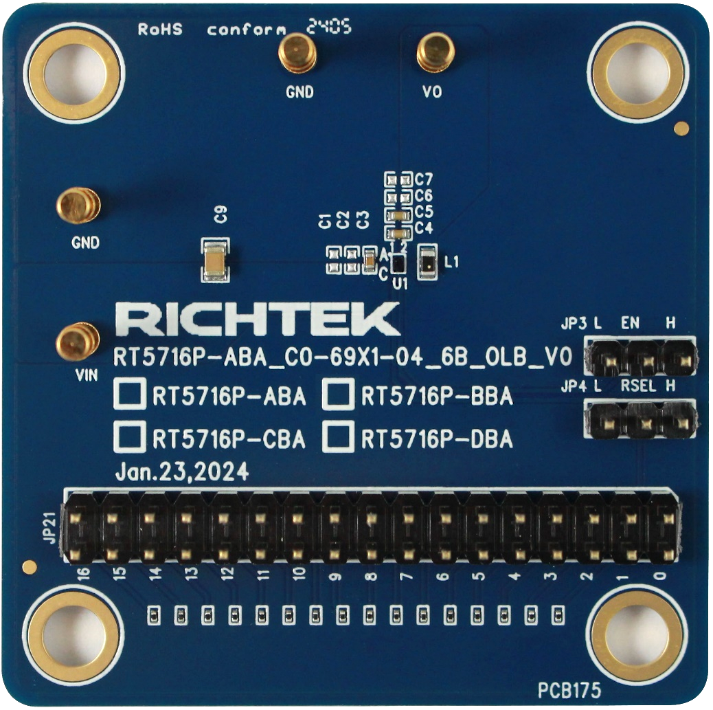
Evaluation Board Layout
Figure 1 to Figure 4 are the RT5716 evaluation board layout for TWL-CSP package. This board size is 84.6mm x 55.7mm and is constructed on four-layer PCB.
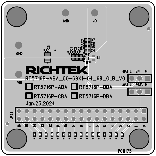
Figure 1. Top View (1st layer)
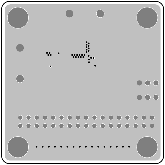
Figure 2. PCB Layout—Inner Side (2nd Layer)
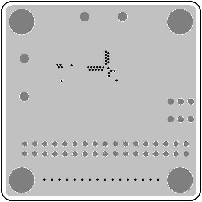
Figure 3. PCB Layout—Inner Side (3rd Layer)
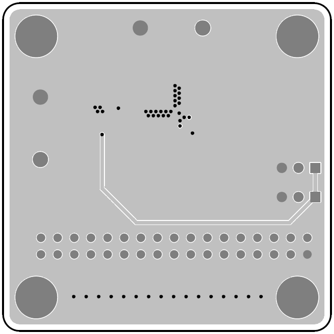
Figure 4. Bottom View (4th Layer)